|
 |
New equipment, processes, materials and etc. which can
realize under 32nm beyond grade critical dimension are demanded
to manufacture highly efficient semiconductor element and resolution in lithography process
must be improved to embody semiconductor technology as mentioned
above.
Research and development for photomask that is essential
material for lithography process must be preceded to realize
resolution enhancement technique, so blankmask which is
core and essential material of photomask must be investigated
and developed. |
|
| The whole quantity
of blankmask has been imported from Japan and Europe and most
from Japan. Accordingly, S&S TECH has started research and
development to target for localization of blankmask from 2001
finished development and research for blankmask background with
superior manpower who gained abundant experience with semiconductor
element and photomask company on June 2002 S&S TECH is
supplying blankmask to home and foreign semiconductor and photomask
company with quality approval. |
 |
| |
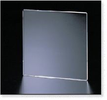
 Quartz Substrate : New Material
 |
|
Cr Layer : Thinner Thickness and New material |
|
Resist Coating : Thinner Thickness and New Resist |
| |
S&S TECH is
steadily recruiting manpower and investing daringly for the goal
of blankmask localization and conducting national policy task
with approval in technology from government and continuously progressing
research and development for next generation blankmask and S&S
TECH will do our best to play an important role of the global
technology leading company.
|
|
|
|